
Multimedia Gallery
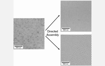
Directed assembly transforms nanoscale disorder (left) into order (right).
Left to its own devices, the "block copolymer" mix used by the University of Wisconsin group will congeal into a disordered pattern resembling a fingerprint (left). But the directed assembly process can transform that pattern into highly ordered stripes or bends (right). These well-aligned geometries are commonly used in the nanofabrication of integrated circuits and microelectronic devices.
Credit: Mark Stoykovich and Paul Nealey
Images credited to the National Science Foundation, a federal agency, are in the public domain. The images were created by employees of the United States Government as part of their official duties or prepared by contractors as "works for hire" for NSF. You may freely use NSF-credited images and, at your discretion, credit NSF with a "Courtesy: National Science Foundation" notation.
Additional information about general usage can be found in Conditions.
Also Available:
Download the high-resolution JPG version of the image. (464 KB)
Use your mouse to right-click (Mac users may need to Ctrl-click) the link above and choose the option that will save the file or target to your computer.
Related story: Self-Assembling Nano-Electronics Turn a Corner