
Center for Optoelectronic Devices, Interconnects, and Packaging (COEDIP)
University of Arizona and the University of Maryland
A National Science Foundation Industry/University Cooperative Research Center since 1984
Partner Institutions:
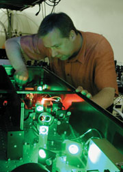
Researchers work to produce useful, innovative, state-of-the-art packaged optoelectronic devices and optical interconnect subsystems
 |
Center Mission and Rationale
The Center is committed to being the leading research and educational Center in the areas of design, fabrication, integration, and packaging of optoelectronic devices and optical interconnects. The Center occupies a special position within the scientific community, with activities spanning the range from fundamental understanding of innovative optical devices to fabrication of optoelectronic devices to activities encompassing integration, packaging, reliability testing, and manufacturing. A unique strength brought about by uniting the University of Arizona and the University of Maryland is the ability to model, fabricate, and package optoelectronic components within the same Center. State-of-the-art fabrication facilities within the two universities allow the fabrication of optoelectronic devices and interconnect subsystems, with packaging occupying center stage from inception to completion of the device/subsystem.
The Center provides a resource base to the scientific community for the development and fabrication of new innovative devices, the understanding of both hybrid and monolithic device integration, and the development of a reproducible and controllable packaging technology.
Research Program
We envision taking advantage of a unique combination of device design expertise and state-of-the-art fabrication and packaging facilities at both universities to fabricate new, innovative devices and optoelectronic subsystems. This collaboration will utilize the resources of the two universities in a synergistic way.
Strategy
- Use our fundamental understanding of devices to design new, innovative devices optimized for a particular application.
- Increase functionality of a component by integration with others.
- Consider packaging as an integral part of device design.
- Perform cross-disciplinary research to refine science, practices, and principles for the design, integration, and packaging of components in a cost-effective and reliable way.
- Provide a forum that fosters a high level of cooperation among the two universities, industry, and government to develop innovative devices and investigate packaging solutions.
- Educate and train future scientists and engineers in an interdisciplinary environment and expose them to industrial practices.
 |
Approach
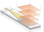
- Focus research on areas of strength within the two universities. These include: research on semiconductor lasers, semiconductor laser amplifiers, and modulators; study of optical nonlinearities of semiconductor and organic compounds; research on optical interconnects; development of unique capabilities such as real-time, in-situ ellipsometry for process control; research on alignment-tolerant structures and silicon bench technology; development of array technology; research on high-performance die attach; integration of optics with electronics using flip-chip bonding; development of advanced components, such as a spectrometer-on-a-chip; and investigation of new characterization tools.
- Develop theoretical models for devices.
- Develop simulation techniques for the integration of different optoelectronic components
- Model the thermal, mechanical, optical, and electrical characteristics of die attach and flip-chip bonding.
- Fabricate demonstration systems that test packaging and device concepts. Several optical interconnect experiments are currently in progress for this purpose.
Special Center Activities
Some examples of the types of devices investigated by the Center are listed below. These examples demonstrate the outstanding device and packaging issues being addressed by the two universities.
- Er-doped fiber amplifiers and lasers
- Glass waveguide amplifiers and lasers
- Organic light emitting diodes for display and lighting
- Semiconductor arrayed waveguide gratings
- Optical connection cube for parallel data transfer
- Low-cost photorefractive polymer devices for 3-D volume holographic storage
- High-power semiconductor laser amplifiers
- Adiabatic beam expansion and alignment-tolerant structures.
Center Headquarters
Center for Optoelectronic Devices, Interconnects, and Packaging
Optical Sciences Center
University of Arizona
Tucson, AZ 85721
Tel (520) 621-4649 * Fax (520) 621-9610
Homepage: www.ee.umd.edu/photonics/COEDIP.htm
Center Co-Director: Nasser Peyghambarian
nnp@u.arizona.edu
Center Co-Director: Aristos Christous
christou@eng.umd.edu
Center Evaluator: David A. Tansik
(520) 621-1710 * dtansik@bpa.arizona.edu
Center Evaluator: Morris S. Ojalvo
(202) 966-8663 * ojalvoms@aol.com
NSF 01-168a