
All Images
Research News
Letting go with lasers

Laser micro-transfer printing constructs micro- and nanocircuits from conventionally fabricated microstructures without contact between these fragile assemblies.
In this illustration of the heart of the process, the laser (red) detaches the nano "ink" (gray) from the stamp (blue) onto the receiving surface (orange). Lasers allow a wider variety of delicate nanostructures to be used in the creation of nanocircuits.
Learn more about lasers at www.nsf.gov/light.Credit: Jorge E. Correa and Placid M. Ferreira, Mechanical Science and Engineering, University of Illinois at Urbana-Champaign
Download the high-resolution PNG version of the image. (390.9 KB)
Use your mouse to right-click (Mac users may need to Ctrl-click) the link above and choose the option that will save the file or target to your computer.
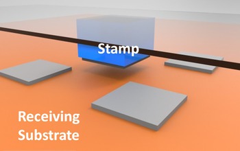
Laser micro-transfer printing constructs micro- and nanocircuits from conventionally fabricated microstructures without contact between these fragile assemblies.
In this illustration showing the beginning of the process, the stamp (blue) with nano "ink" (gray) goes to position over the receiving surface (orange).Credit: Jorge E. Correa and Placid M. Ferreira, Mechanical Science and Engineering, University of Illinois at Urbana-Champaign
Download the high-resolution PNG version of the image. (425.7 KB)
Use your mouse to right-click (Mac users may need to Ctrl-click) the link above and choose the option that will save the file or target to your computer.

Laser micro-transfer printing constructs micro- and nanocircuits from conventionally fabricated microstructures without contact between these fragile assemblies.
In this illustration of the end of the process, the stamp (blue) has released the nano "ink" (grey) onto the receiving surface (orange), where the nanostructures and substrate together can form circuits due to their different electrical properties.Credit: Jorge E. Correa and Placid M. Ferreira, mechanical science and engineering, University of Illinois at Urbana-Champaign
Download the high-resolution PNG version of the image. (368.5 KB)
Use your mouse to right-click (Mac users may need to Ctrl-click) the link above and choose the option that will save the file or target to your computer.
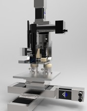
Placid Ferreira of the Univeristy of Illinois at Urbana-Champaign enlists lasers to help manufacture objects too small for the human eye to see. The laser micro-transfer printer makes it possible to use a wider range of materials in nanomanufacturing.
Ferreira's printer's high-resolution vertical optical column allows precision alignment of the stamp and application of the laser beam, while the lower part has adjustable tilt angles for the surface that receives nano "ink" from the stamp.
Learn more about advanced manufacturing at www.nsf.gov/madetoorder.Credit: Placid M. Ferreira, Mechanical Science and Engineering, University of Illinois at Urbana-Champaign.
Download the high-resolution PNG version of the image. (118.6 KB)
Use your mouse to right-click (Mac users may need to Ctrl-click) the link above and choose the option that will save the file or target to your computer.