
Multimedia Gallery
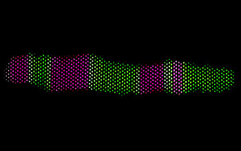
Transformation of an HfO2 nanorod
A collaborative team of researchers observed in real-time the transformation of an HfO2 nanorod from its room temperature to tetragonal phase at 1000 degrees less than its bulk temperature. Nanorod surfaces and twin boundary defects (pictured here) serve to kinetically trap this phase.
More about this image
A team of researchers led by chemists Beth Guiton of the University of Kentucky and Sarbajit Banerjee of Texas A&M University, working in collaboration with Texas A&M materials science engineer Raymundo Arroyave, has found a way to achieve this highly sought tetragonal phase at 1100 degrees Fahrenheit -- think much closer to room temperature and a potential holy grail for the computing industry, along with countless other sectors and applications.
In a published paper about their research, the team details their observation of this spectacular atom-by-atom transformation, witnessed with the help of incredibly powerful microscopes at Oak Ridge National Laboratory. After first shrinking monoclinic hafnium dioxide particles down to the size of tiny crystal nanorods, the researchers gradually heated them, paying close attention to the barcode-like structure characterizing each nanorod and, in particular, its pair of nanoscale, fault-forming stripes that seem to function as ground zero for the transition.
"In this study we are watching a tiny metal oxide rod transform from one structure, which is the typical material found at room temperature, into a different, related structure not usually stable below 3100 degrees Fahrenheit," said Guiton, who is an associate professor of chemistry in the UK College of Arts & Sciences. "This is significant because the high-temperature material has amazing properties that make it a candidate to replace silicon dioxide in the semiconductor industry, which is built on silicon."
As computer chips become smaller, faster and more powerful, their insulating layers must also be much more robust -- currently a limiting factor for semiconductor technology. Guiton says this new phase of hafnia is an order of magnitude better at withstanding applied fields.
[This research was supported in part by the National Science Foundation (grants DMR 14-55154, DMR 15-04702 and CMMI 15-34534).]
To learn more about this research, see the NSF News From the Field story Hafnia dons a new face: Materials research creates potential for improved computer chips and transistors. (Date image taken: May 2017; date originally posted to NSF Multimedia Gallery: May 30, 2018)
Credit: Bethany Hudak, University of Kentucky
Images and other media in the National Science Foundation Multimedia Gallery are available for use in print and electronic material by NSF employees, members of the media, university staff, teachers and the general public. All media in the gallery are intended for personal, educational and nonprofit/non-commercial use only.
Images credited to the National Science Foundation, a federal agency, are in the public domain. The images were created by employees of the United States Government as part of their official duties or prepared by contractors as "works for hire" for NSF. You may freely use NSF-credited images and, at your discretion, credit NSF with a "Courtesy: National Science Foundation" notation.
Additional information about general usage can be found in Conditions.
Also Available:
Download the high-resolution JPG version of the image. (1.8 MB)
Use your mouse to right-click (Mac users may need to Ctrl-click) the link above and choose the option that will save the file or target to your computer.