
Multimedia Gallery
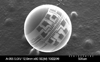
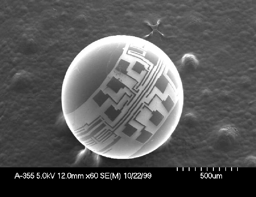
Ball Semiconductor (Image 2)
A spherical semiconductor and microelectromechanical systems (MEMS) device technology.
The unique technology was the foundation for which Ball Semiconductor Inc. (Allen, Texas) was created. While the technology has an obvious advantage of having a larger available surface area in a given footprint, the development of its materials, processes, device designs and fabrication methods have led to numerous new findings.
Ball semiconductor device development efforts have been concentrated in five key technology areas: single-crystal sphere fabrication, non-contact process methods, lithographic techniques, design protocols and assembly methods. While its unique, single-crystal manufacturing method has led to a new breakthrough in fabricating materials in other applications and industries, many new sensor device technologies have also been discovered to enable a much wider range and more accurate measurement than what was conventionally possible. Additionally, its unique processing techniques have demonstrated new potential in multiple ball stacks, new bonding and bumping technologies, and new production environment designs.
One of the key elements, the lithography techniques to patter around the curved surface directly from the device design's CAD data, has developed into its own technology to provide high-resolution, direct imaging solutions to benefit other applications and industries such as PCB, HDI-packaging, FPD and MEMS fabrication. (Date of Image: unknown) [See Related Image.]
SORRY: THIS IMAGE IS NOT AVAILABLE IN HIGH-RESOLUTION FORMAT
Credit: Research and photo by component technology group at Ball Semiconductor Inc. (U.S. Pat. 5,955,776); Akira Ishikawa (Founder)--spherical shaped semiconductor integrated circuit
Images and other media in the National Science Foundation Multimedia Gallery are available for use in print and electronic material by NSF employees, members of the media, university staff, teachers and the general public. All media in the gallery are intended for personal, educational and nonprofit/non-commercial use only.
Images credited to the National Science Foundation, a federal agency, are in the public domain. The images were created by employees of the United States Government as part of their official duties or prepared by contractors as "works for hire" for NSF. You may freely use NSF-credited images and, at your discretion, credit NSF with a "Courtesy: National Science Foundation" notation.
Additional information about general usage can be found in Conditions.
Also Available:
Download the high-resolution JPG version of the image. (204 KB)
Use your mouse to right-click (Mac users may need to Ctrl-click) the link above and choose the option that will save the file or target to your computer.