
Multimedia Gallery

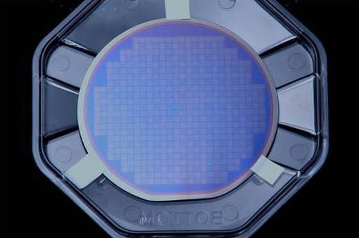
Wafer-scale nanopatterning may be used in the fabrication of LED structures.
Wafer-scale nanopatterning is used in the fabrication of photonic crystal structures for light emitting diodes or LEDs. Creating nanomanufacturing process systems that are high-throughput, reliable and versatile is the focus of the NSF Nanosystems Engineering Research Center led by the University of Texas, called the Center for Nanomanufacturing Systems for Mobile Computing and Mobile Energy Technologies or NASCENT.
Credit: Cockrell School of Engineering, University of Texas at Austin
See other images like this on your iPhone or iPad download NSF Science Zone on the Apple App Store.
Images credited to the National Science Foundation, a federal agency, are in the public domain. The images were created by employees of the United States Government as part of their official duties or prepared by contractors as "works for hire" for NSF. You may freely use NSF-credited images and, at your discretion, credit NSF with a "Courtesy: National Science Foundation" notation.
Additional information about general usage can be found in Conditions.
Also Available:
Download the high-resolution JPG version of the image. (123 KB)
Use your mouse to right-click (Mac users may need to Ctrl-click) the link above and choose the option that will save the file or target to your computer.
Related story: Engineering Research Centers Awarded $55.5M to Innovate in Nanoscale Science and Engineering