
News Release 05-075
Silicon Solution Could Lead to a Truly Long-life Battery
New devices may provide power for decades

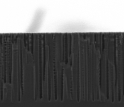
The wafer test fixture the researchers used to test the new porous-silicon diode.
May 10, 2005
This material is available primarily for archival purposes. Telephone numbers or other contact information may be out of date; please see current contact information at media contacts.
Using some of the same manufacturing techniques that produce microchips, researchers have created a porous-silicon diode that may lead to improved betavoltaics. Such devices convert low levels of radiation into electricity and can have useful lives spanning several decades.
While producing as little as one-thousandth of the power of conventional chemical batteries, the new "BetaBattery" concept is more efficient and potentially less expensive than similar designs and should be easier to manufacture. If the new diode proves successful when incorporated into a finished battery, it could help power such hard-to-service, long-life systems as structural sensors on bridges, climate monitoring equipment and satellites.
The battery's staying power is tied to the enduring nature of its fuel, tritium, a hydrogen isotope that releases electrons in a process called beta decay. The porous-silicon semiconductors generate electricity by absorbing the electrons, just as a solar cell generates electricity by absorbing energy from incoming photons of light.
Supported by grants from the NSF Small Business Innovation Research (SBIR) program, a multi-disciplinary team of researchers from the University of Rochester, the University of Toronto, Rochester Institute of Technology and BetaBatt, Inc. of Houston, Texas, describe their new diode in the May 13 issue of Advanced Materials.
Researchers have been attempting to convert various types of radiation into electricity since the development of the transistor more than 50 years ago. Mastering the junctions between relatively electron-rich and electron-poor regions of semiconductor material (p-n junctions) led to many modern electronic products.
Yet, while engineers have been successful at capturing electromagnetic radiation with solar cells, the flat, thin devices have been unable to collect enough beta-decay electrons to yield a viable betavoltaic device.
The BetaBatt will not be the first battery to harness a radioactive source, or even the first to use tritium, but the new cell will have a unique advantage - the half-millimeter-thick silicon wafer into which researchers have etched a network of deep pores. This structure vastly increases the exposed surface area, creating a device that is 10 times more efficient than planar designs.
"The 3-D porous silicon configuration is excellent for absorbing essentially all the kinetic energy of the source electrons," says co-author Nazir Kherani of the University of Toronto. Instead of generating current by absorbing electrons at the outermost layer of a thin sheet, surfaces deep within these porous silicon wafers accommodate a much larger amount of incoming radiation. In early tests, nearly all electrons emitted during the tritium's beta decay were absorbed.
There were a number of practical reasons for selecting tritium as the source of energy, says co-author and patent holder Larry Gadeken of BetaBatt - particularly safety and containment.
"Tritium emits only low energy beta particles (electrons) that can be shielded by very thin materials, such as a sheet of paper," says Gadeken. "The hermetically-sealed, metallic BetaBattery cases will encapsulate the entire radioactive energy source, just like a normal battery contains its chemical source so it cannot escape."
Even if the hermetic case were to be breached, adds Gadeken, the source material the team is developing will be a hard plastic that incorporates tritium into its chemical structure. Unlike a chemical paste, the plastic cannot not leak out or leach into the surrounding environment.
Researchers and manufacturers have been producing porous silicon for decades, and it is commonly used for antireflective coatings, light emitting devices, and photon filters for fiber optics. However, the current research is the first patented betavoltaic application for porous silicon and the first time that 3-D p-n diodes have been created with standard semiconductor industry techniques.
"The betavoltaic and photovoltaic applications of 3-D porous silicon diodes will result in an exciting arena of additional uses for this versatile material," says co-author Philippe Fauchet of the University of Rochester.
"This is the first time that uniform p-n junctions have been made in porous silicon, which is exciting from the point of view of materials science," says Fauchet. For example, because of its characteristics and photon sensitivity, each diode pore could serve as an individual detector, potentially creating an extremely high-resolution image sensor.
"The ease of using standard semiconductor processing technology to fabricate 3-D p-n junctions was surprising," adds co-author Karl Hirschman of the Rochester Institute of Technology. That manufacturing ease is an important breakthrough for increasing production and lowering costs, and it makes the device scalable and versatile for a range of applications.
"The initial applications will be for remote or inaccessible sensors and devices where the availability of long-life power is critical," says Gadeken.
The BetaBattery may prove better suited to certain tasks than chemical batteries when power needs are limited. The structures are robust--tolerant to motion and shock, and functional from -148° Fahrenheit (-100° Celsius) to 302° F (150°C)--and may never have to be changed for the lifetime of the device.
-NSF-
-
A scanning electron micrograph of the side view of the porous-silicon wafer.
Credit and Larger Version -
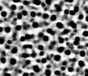
A scanning electron micrograph of the top view of the porous-silicon wafer.
Credit and Larger Version
Article reference: (W. Sun et al., Adv. Mater. 2005, 17, 1230.)
The NSF Engineering Directorate's SBIR and Small Business Technology Transfer (STTR) programs target small businesses and their partners at universities, enabling the companies to pursue high-risk science and engineering research that could one day prove both useful and economically valuable. One area of investment is alternative electricity-generation technology, such as BetaBatt. In fiscal year 2004, NSF provided just over $100 million to support small business programs.
Gadeken SBIR Phase I & II Awards: NSF Award No. 0320029: A Semiconductor Device for Direct and Efficient Conversion of Radioisotope Energy http://www.nsf.gov/awardsearch/showAward.do?AwardNumber=0320029
Media Contacts
Joshua A. Chamot, NSF, (703) 292-7730, email: jchamot@nsf.gov
Karen Kelly, University of Toronto, (416) 978- 6974, email: k.kelly@utoronto.ca
Michael Saffran, Rochester Institute of Technology, (585) 475-5697, email: mjsuns@rit.edu
Jonathan Sherwood, University of Rochester, (585) 273-4726, email: jonathan.sherwood@rochester.edu
Program Contacts
T. James Rudd, NSF, (703) 292-4759, email: tjrudd@nsf.gov
Principal Investigators
Larry Gadeken, BetaBatt, Inc., (xxx) xxx-xxxx, email: info@betabatt.com
The U.S. National Science Foundation propels the nation forward by advancing fundamental research in all fields of science and engineering. NSF supports research and people by providing facilities, instruments and funding to support their ingenuity and sustain the U.S. as a global leader in research and innovation. With a fiscal year 2023 budget of $9.5 billion, NSF funds reach all 50 states through grants to nearly 2,000 colleges, universities and institutions. Each year, NSF receives more than 40,000 competitive proposals and makes about 11,000 new awards. Those awards include support for cooperative research with industry, Arctic and Antarctic research and operations, and U.S. participation in international scientific efforts.
Connect with us online
NSF website: nsf.gov
NSF News: nsf.gov/news
For News Media: nsf.gov/news/newsroom
Statistics: nsf.gov/statistics/
Awards database: nsf.gov/awardsearch/
Follow us on social
Twitter: twitter.com/NSF
Facebook: facebook.com/US.NSF
Instagram: instagram.com/nsfgov