

Get OLPA Email Updates
The Office of Legislative and Public Affairs (OLPA) communicates the U.S. National Science Foundation's activities, programs, research results and policies.
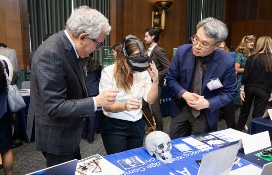
OLPA uses a variety of approaches to engage with the public, Congress, the news media, state and local governments, other federal agencies, research and education communities and internal NSF offices and directorates.
OLPA branches
Government Affairs
The Government Affairs branch is the principal point of contact between Congress and NSF, coordinating requests for information and ensuring timely responses to congressionally mandated reports and correspondence. The branch also arranges meetings with congressional members and staff, coordinates NSF officials' appearances at congressional hearings and arranges site visits to NSF-supported facilities.
Visit the NSF and Congress webpage for information on the latest budget request to Congress, congressional testimonies and summaries, major legislation and program awards by state/district.
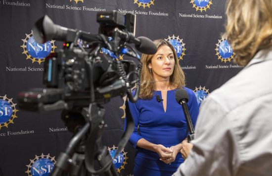
External Affairs
The External Affairs branch leads external communications for the agency, including planning and strategy, media relations, digital engagement, brand management, content development and outreach.
For media inquiries, please call (703) 292-7090 or email media@nsf.gov.
For questions about NSF branding or logo usage, email nsfbranding@nsf.gov.