


Credit: Ryan Hoover, Electrical & Computer Engineering, University of Washington
Download a high-resolution version of this image (JPEG, 1.4MB)
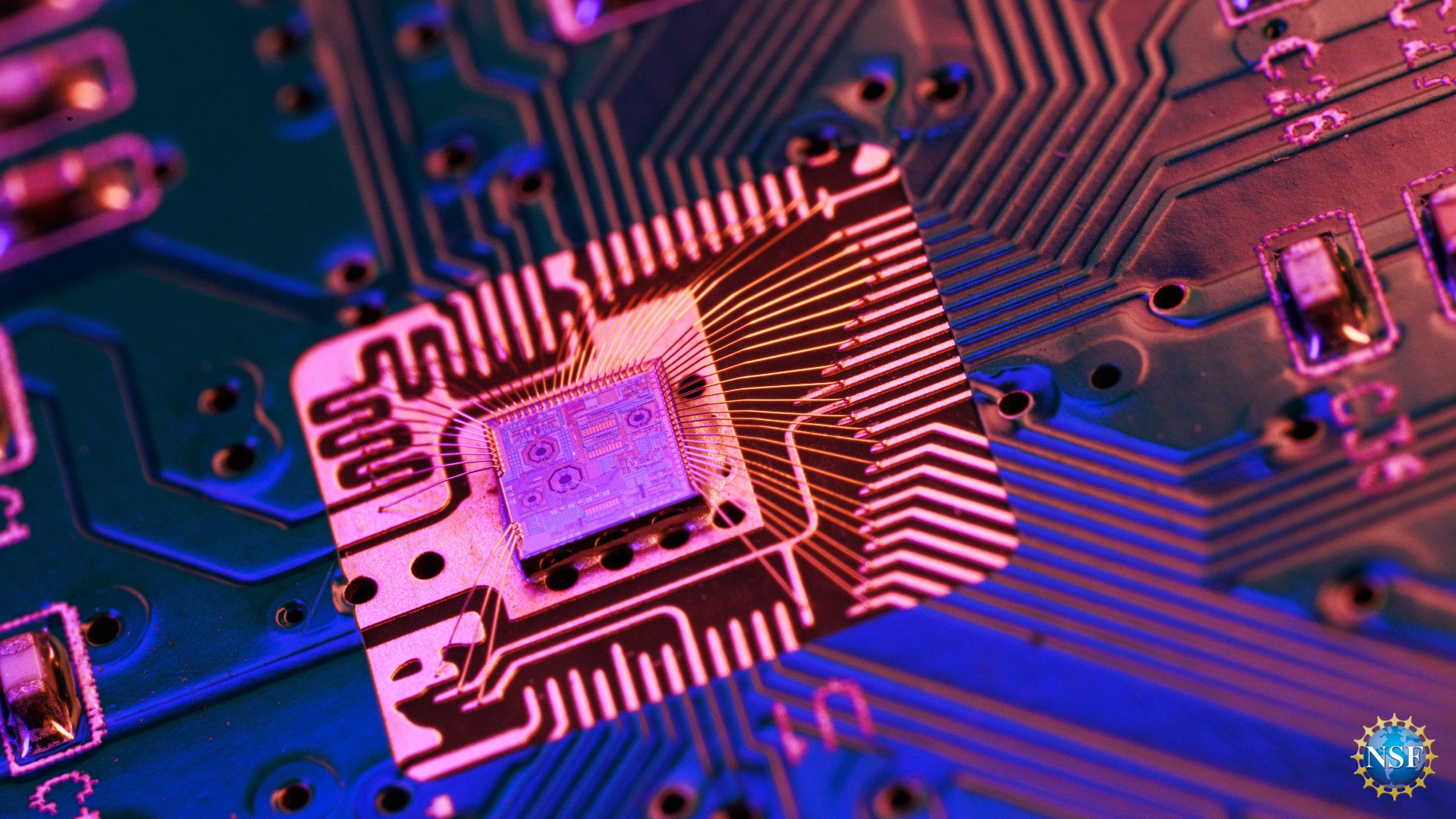

Credit: Jun Liu, North Carolina State University
Download a high-resolution version of this image (JPEG, 0.9MB)


Credit: Ella Maru Studio
Download a high-resolution version of this image (JPEG, 2MB)
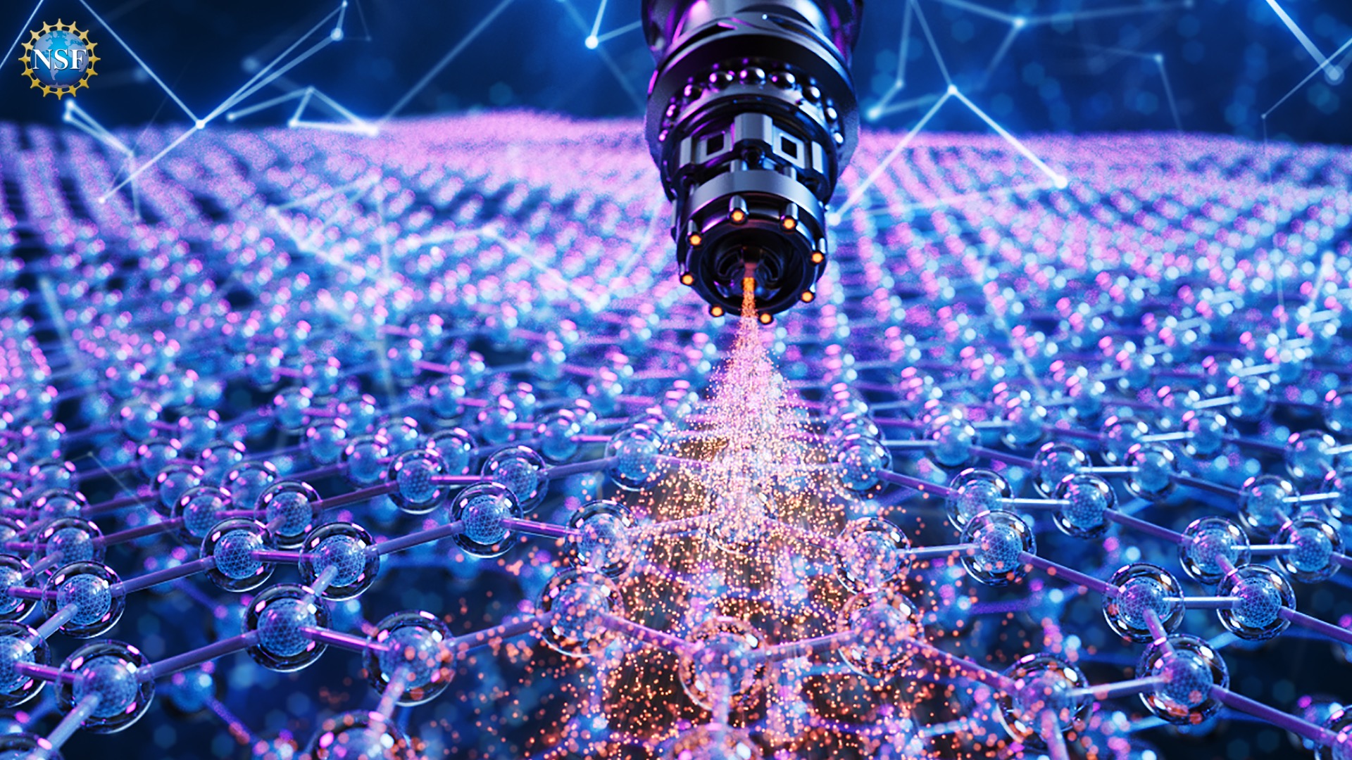

Credit: Chris Coleman, School of Computing, University of Utah
Download a high-resolution version of this image (JPEG, 2.1MB)


Credit: Ryan Hoover, Electrical & Computer Engineering, University of Washington
Download a high-resolution version of this image (JPEG, 1MB)


Credit: Ayar Labs
Download a high-resolution version of this image (JPEG, 1.5MB)


Credit: P. Roushan\Martinis lab\UC Santa Barbara
Download a high-resolution version of this image (JPEG, 2.2MB)